Semiconductor Electronics: Materials, Devices and Simple Circuits Class 12 MCQ Questions with Answers
MCQ On Semiconductor Class 12 Chapter 14 Question 1.
In an n-type silicon, which of the following statement is true:
(A)Electrons are majority carriers and trivalent atoms are the dopants.
(B)Electrons are minority carriers and pentavalent atoms are the dopants.
(C)Holes are minority carriers and pentavalent atoms are the dopants.
(D)Holes are majority carriers and trivalent atoms are the dopants.
Answer:
(C)Holes are minority carriers and pentavalent atoms are the dopants.
Explanation:
In an n-type silicon the holes are the minority carriers. An n-type semiconductor is obtained when pentavalent atoms, such as phosphorus, are doped in silicon atoms.
![]()
Semiconductor Class 12 MCQ Chapter 14 Question 2.
In an n-type silicon, which of the following statement is true for p-type semiconductors?
(A)Electrons are majority carriers and trivalent atoms are the dopants.
(B)Electrons are minority carriers and pentavalent atoms are the dopants.
(C)Holes are minority carriers and pentavalent atoms are the dopants.
(D)Holes are majority carriers and trivalent atoms are the dopants.
Answer:
(D)Holes are majority carriers and trivalent atoms are the dopants.
Explanation:
In a p-type semiconductor, the holes are the majority carriers, while the electrons are the minority carriers. A p-type semiconductor is obtained when trivalent atoms, such as aluminium, are doped in silicon atoms.
Semiconductor MCQ Class 12 Chapter 14 Question 3.
Carbon, silicon and germanium have four valence electrons each. These are characterised by valence and conduction bands separated by energy band gap respectively equal to (Eg)C, (Eg, )Si and (Eg)Ge Which of the following statements is true?
(A) (Eg)Si < (Eg)Ge < (Eg)C
(B) (Eg)C < (Eg)Ge > (Eg)Si
(C) (Eg)C > (Eg)Si >(Eg)Ge
(D) (Eg)C = (Eg )Si = (Eg)Ge
Answer:
(C) (Eg)C > (Eg)Si >(Eg)Ge
Explanation:
Above mentioned three given elements, the energy band gap of carbon is the maximum and that of germanium is the least. The energy band gaps of these elements are related as:
(Eg)C > (Eg)Si >(Eg)Ge
![]()
Chapter 14 Physics Class 12 MCQs Question 4.
The conductivity of a semiconductor increases with increase in temperature because
(A) number density of free current carriers increases.
(B) relaxation time increases.
(C) both number density of carriers and relaxation time increase.
(D) number density of current carriers increases; relaxation time decreases but effect of decrease in relaxation time is much less than the increase in number density.
Answer:
(D) number density of current carriers increases; relaxation time decreases but effect of decrease in relaxation time is much less than the increase in number density.
Explanation:
In semiconductor, the density of charge carriers (electron, holes) are very small, so its resistance is high. When temperature increases, the charge carriers (density) increases which increases the conductivity. As temperature of semiconductor increases, the speed of free electrons increases which decreases the relaxation time. As the density of charge carrier is small, so there is small effect on decrease of relaxation time.
Class 12 Semiconductor MCQ Chapter 14 Question 5.
Hole is …………
(A)an anti-particle of electron.
(B)a vacancy created when an electron leaves a covalent bond.
(C)absence of free electrons.
(D)an artificially created particle.
Answer:
(B)a vacancy created when an electron leaves a covalent bond.
Explanation:
Atoms of semiconductor are binding by covalent bonds between the atoms of same or different type. Due to thermal agitation when an electron leaves its position and become free, it leaves a vacancy of electron and this vacancy in the bond (covalent) is called hole.
![]()
Semiconductor MCQ Questions And Answers Pdf Class 12 Question 6.
Semiconductors behave like insulators at
(A) 0°C
(B) 0 K
(C) 273 K
(D) None of the above
Answer:
(B) 0 K
Explanation:
At 0 K temperature, all electrons of semiconductor are immovable from their shell as they do not have sufficient energy. So no free electron is available as charge carrier. This make the insulators to behave like insulators.
Electronics Physics MCQs Chapter 14 Class 12 Question 7.
When the conductivity of a semiconductor is due to rupture of its covalent bond only then the semiconductor is called ……..
(A) Intrinsic
(B) Extrinsic
(C) Donor
(D) acceptor
Answer:
(A) Intrinsic
Explanation:
In intrinsic semiconductor, conductivity increases with rise of temperature due to rupture of covalent bonds and thus charge carriers become available. In extrinsic semiconductor, conductivity increases due to doping and also due to rupture of covalent bonds with rise of temperature.
Question 8.
Tetra valent semiconductor is to be doped with valent element to achieve type extrinsic semiconductor.
(A) penta, n
(B) tri, p
(C) penta, p
(D) both (A) and (B)
Answer:
(D) both (A) and (B)
Explanation:
When a semiconductor having 4 valence electrons is doped with an element having 3 valence electrons, then an excess hole is generated and the semiconductor becomes p-type extrinsic semiconductor.
When a semiconductor having 4 valence electrons is doped with an element having 5 valence electrons, then an excess electron becomes available and the semiconductor becomes n-type extrinsic semiconductor.
![]()
Question 9.
In an unbiased p-n junction, holes diffuse from the p-region to n-region because
(A) free electrons in the n-region attract them.
(B) they move across the junction by the potential difference.
(C) hole concentration in p-region is more as compared to n-region.
(D) All the above.
Answer:
(C) hole concentration in p-region is more as compared to n-region.
Explanation:
The diffusion of charge carriers across a junction takes place from the regions of higher concentration to lower concentration. In this case, the p-region has greater concentration of holes than the n-region. Hence, in an unbiased p-n junction, holes diffuse from the p-region to the n-region.
Question 10.
When a forward bias is applied to a p-n junction, it ……..
(A) raises the potential barrier.
(B) reduces the majority carrier current to zero.
(C) lowers the potential barrier.
(D) None of the above
Answer:
(C)lowers the potential barrier.
Explanation:
When a forward bias is applied to a p-n junction, it lowers the value of potential barrier. In the case of a forward bias, the potential barrier opposes the applied voltage. Hence, the potential barrier across the junction gets reduced.
Question 11.
In Figure, V0 is the potential barrier across a p-n junction, when no battery is connected across the junction
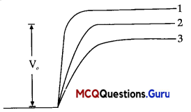
(A) 1 and 3 both correspond to forward bias of junction
(B) 3 corresponds to forward bias of junction and 1 corresponds to reverse bias of junction
(C) 1 corresponds to forward bias and 3 corresponds to reverse bias of junction.
(D) 3 and 1 both correspond to reverse bias of junction.
Answer:
(B) 3 corresponds to forward bias of junction and 1 corresponds to reverse bias of junction
Explanation:
When p-n junction is in forward bias, it compresses or decreases the depletion layer, due to which potential barrier in forward bias decreases and in reverse bias potential barrier increases.
![]()
Question 12.
In Figure, assuming the diodes to be ideal,
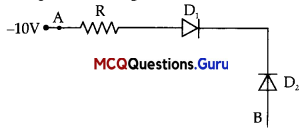
(A) D1 is forward biased and D2 is reverse biased and hence current flows from A to B
(B) D2 is forward biased and D1 is reverse biased and hence no current flows from B to A and vice versa.
(C) D1 and D2 are both forward biased and hence current flows from A to B.
(D) D1 and D2 are both reverse biased and hence no current flows from A to B and vice versa.
Answer:
(B) D2 is forward biased and D1 is reverse biased and hence no current flows from B to A and vice versa.
Explanation:
In circuit, A is at -10 V and B is at 0 V So B is positive than A. So D2 is in forward bias and D1 is in reverse bias, so no current flows from A to B or B to A.
Question 13.
A 220 V A.C. supply is connected between points A and B in Figure. What will be the potential difference V across the capacitor?
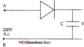
(A) 220 V
(B) 110V
(C) 0V
(D) \(220 \sqrt{2}\) V
Answer:
(D) \(220 \sqrt{2}\) V
Question 14.
The output of the given circuit in Figure
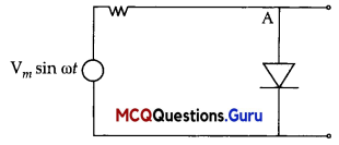
(A) would be zero at all times.
(B) would be like a half wave rectifier with positive cycles in output.
(C) would be like a half wave rectifier with negative cycles in output.
(D) would be like that of a full wave rectifier.
Answer:
(C) would be like a half wave rectifier with negative cycles in output.
Explanation:
When positive cycle is at A, diode will be in forward bias and resistance due to diode is approximately zero so potential across diode will be about zero.
Similarly, when there is negative half cycle at A, diode will be in reverse bias and resistance will be maximum so potential difference across diode is V sin of with negative at A. So we get only negative output at A, so it behaves like a half-wave rectifier with negative cycle at A in output, verifies the answer (C).
![]()
Question 15.
In the circuit shown in Figure, if the diode forward voltage drop is 0.3 V, the voltage difference between A and B is
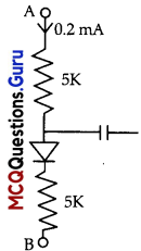
(A) 1.3 V
(B) 2.3 V
(C)0V
(D) 0.5 V
Answer:
(B) 2.3 V
Explanation:
In the middle right of the circuit the capacitor behaves like an open circuit for dc 0.2 mA current, so current will flow from A to B only. Let potential across A and B is V, so by Kirchhoff’s loop law,
VAB = (5,000 × 0.2 × 10-3) + 0.3 + 5,000 × 0.2 × 10-3
VAB = 1 V + 0.3 V + 1 V
VAB = 2.3 V
Question 16.
Which one of the following diagrams depicts the proper flow or electrons and holes in a forward biased p-n junction diode?
(A)
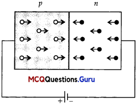
(B)
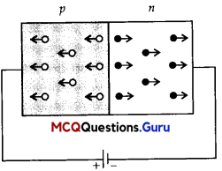
(C)
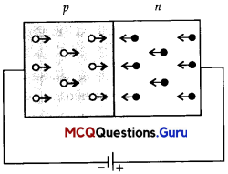
(D)
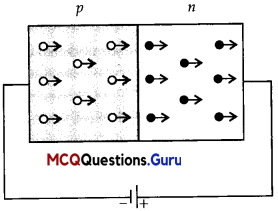
Answer:
Explanation:
In a forward biased p-n junction diode, the positive terminal of the battery is connected to the p-side and negative terminal of the battery is connected to the n-side of the diode. Holes flow from p-side to n-side and electrons flow from n-side to p-side.
![]()
Assertion And Reason Based MCQs (1 Mark each)
Directions: In the following questions, A statement of Assertion (A) is followed by a statement of Reason (R). Mark the correct choice as.
(A) Both A and R are true and R is the correct explanation of A
(B) Both A and R are true but R is NOT the correct explanation of A
(C) A is true but R is false
(D) A is false and R is true
Question 1.
Assertion (A): The number of electrons in a p-type silicon semiconductor is less than the number of electrons in intrinsic silicon semiconductor at room temperature.
Reason (R): It is due to law of mass action.
Answer:
(A) Both A and R are true and R is the correct explanation of A
Explanation:
In p-type semiconductor, electron is the minority charge carrier. So, number of electrons is less than the number of electrons in intrinsic semiconductor. So the assertion is true. According to the law of mass action = n-2i= ne × nh. In intrinsic semiconductor, ne = nh. So in p-type semiconductor, ne < nh. So reason is also true.
Question 2.
Assertion (A): The resistivity of a semiconductor decreases with temperature.
Reason (R): The atoms of a semiconductor vibrate with larger amplitude at higher temperature there by increasing it’s resistivity.
Answer:
(D) A is false and R is true
Explanation:
Resistivity of semiconductors decreases with temperature. So, assertion is true. Electrons from valence band jumps to conduction band with rise of temperature and hence the resistivity decreases. Hence, the reason is also false.
![]()
Question 3.
Assertion (A): As the temperature of a semiconductor increases, its resistance decreases.
Reason (R): The energy gap between conduction band and valence band is small.
Answer:
(A) Both A and R are true and R is the correct explanation of A
Explanation:
As temperature rises, the electrons of valence band sufficient energy and jump to conduction band. Thus, the resistivity decreases. So assertion is true.
In semiconductors the energy gap between conduction band and valence band is small. Due to this, the electrons in conduction band can gain sufficient thermal energy with temperature rise and can easily jump across the small energy gap to reach conduction band. Thus, conductivity increased and resistance decreases.
Question 4.
Assertion (A): Silicon is preferred over Germanium for making semiconductor devices.
Reason (R): The energy gap of Germanium is more than the energy gap of Silicon.
Answer:
(B) Both A and R are true but R is NOT the correct explanation of A
Explanation:
Silicon is preferred over Germanium for making semiconductor devices. The assertion is true. The energy gap of Germanium is about 0.7 eV, where as the energy gap of Silicon is 1.1 eV. Hence, the reason is false.
Question 5.
Assertion (A): Semiconductors do not obey Ohm’s law.
Reason (R): V-I characteristic of semiconductors is linear.
Answer:
(C) A is true but R is false
Explanation:
Semiconductors do not obey Ohm’s law. So the assertion is true. V-I characteristic of semiconductor is non-linear. Hence the reason is false.
Question 6.
Assertion (A): Zenger diode is used as a voltage regulator.
Reason (R): Zenger diode operated in reverse biased condition.
Answer:
(B) Both A and R are true but R is NOT the correct explanation of A
Explanation:
Zener diode is used as a voltage regulator in reverse biased condition. So, both assertion and reason are true, but the reason does not explain the assertion.
![]()
Question 7.
Assertion (A): Ideal diode shows zero resistance in forward bias and infinite resitance in reverse bias.
Reason (R): Depletion region of a p-n junction diode extends in reverse bias and contracts in reverse bias.
Answer:
(A) Both A and R are true and R is the correct explanation of A
Explanation:
In forward bias condition, the depletion region of a p-n junction diode contracts and the majority charge carriers can cross the junction very easily. So, the resistance becomes low (ideally 0).
In reverse bias condition, the depletion region of p-n junction diode expands and the majority charge carriers cannot cross the junction. So, the resistance increases (ideally o). So, the assertion and reason both are true and reason explains the assertion.
Question 8.
Assertion (A): When diode is used as a rectifier, its specified reverse breakdown voltage should not be exceeded.
Reason (R): When p-n junction diode crosses the reverse break down voltage, it get destroyed.
Answer:
(A) Both A and R are true and R is the correct explanation of A
Explanation:
When a diode is used as a rectifier, it has to face both positive and negative halves of the alternating voltage. Care is taken so that the amplitude of the negative half cycle of the alternating voltage should not be more than the specified reverse breakdown voltage of the diode. So the assertion is true.
Reverse break down voltage of normal p-n junction diodes used as a rectifier is high. If reverse voltage exceeds this specified break down voltage, then the diode gets permanently damaged. So, the reason is also true and explains the assertion.
![]()
Question 9.
Assertion (A): When a p-n junction diode is reverse biased, a feeble reverse current flows known as reverse saturation current.
Reason (R): In reverse bias condition, the minority carries can cross the junction.
Answer:
(A) Both A and R are true and R is the correct explanation of A
Explanation:
When a p-n junction is reverse biased, then the majority charge carriers cannot cross the junction. So, no forward current flows. But in reverse direction, a feeble current flows which is known as reverse saturation current. So, the assertion is true. In p-side there are few electrons as minority charge carrier and in n-side, there are few holes as minority charge carriers.
In reverse bias condition, the holes at n-side feel a pull exerted by the negative polarity of the voltage source connected to the p-side. Similarly, the electrons at p-side feel a pull exerted by the positive polarity of the voltage source connected to the n-side. So, these minority carries now can cross the junction and give rise to a feeble current in the opposite direction. Hence, the reason is also true and it explains the assertion.
Case Based MCQs
Attempt any 4 sub-parts out of 5. Each sub-part carries 1 mark.
I. Read the following text and answer the following questions on the basis of the same:
Band theory of solid:
Consider that the Si or Ge crystal contains N atoms. Electrons of each atom will have discrete energies in different orbits. The electron energy will be same if all the atoms are isolated, i.e., separated from each other by a large distance. However, in a crystal, the atoms are close to each other (2 A to 3 A) and therefore the electrons interact with each other and also with the neighbouring atomic cores.
The overlap (or interaction) will be more felt by the electrons in the outermost orbit while the inner orbit or core electron energies may remain unaffected. Therefore, for understanding electron energies in Si or Ge crystal, we need to consider the changes in the energies of the electrons in the outermost orbit only. For Si, the outermost orbit is the third orbit (n = 3), while for Ge it is the fourth orbit (n = 4)
The number of electrons in the outermost orbit is 4 (2s and 2p electrons). Hence, the total number of outer electrons in the crystal is 4N. The maximum possible number of outer electrons in the orbit is 8 (2s + 6p electrons). So, out of the 4N electrons, 2N electrons are in the 2N s-states (orbital quantum number l = 0) and 2N electrons are in the available 6N p-states. Obviously, some p-electron states are empty. This is the case of well separated or isolated atoms.
Question 1.
The energy of electrons of atoms of a substance will be same if:
(A) atoms are isolated.
(B) atoms are closely spaced.
(C) atoms are excited.
(D) atoms are charged.
Answer:
(A) atoms are isolated.
Explanation:
The electron energy will be same if all the atoms are isolated, i.e., separated from each other by a large distance.
![]()
Question 2.
In a crystal, the distance between two atoms is:
(A) 200 A to 300 A
(B) 2 A to 3 micron
(C) 2 A to 3 A
(D) 2 mm to 3 mm
Answer:
(C) 2 A to 3 A .
Explanation:
In a crystal, the atoms are dosed to each other (2 A to 3 A).
Question 3.
The overlap (or interaction) will be more felt by the electrons when they are:
(A) in the outermost orbit.
(B) in the innermost orbit.
(C) free.
(D) in any orbit.
Answer:
(A) in the outermost orbit.
Explanation:
The overlap (or interaction) will be more felt by the electrons in the outermost orbit, while the inner orbit or core electron energies may remain unaffected.
Question 4.
For Silicon and Germanium the outermost orbits are respectively:
(A) n = 3 and n = 5
(B) n = 4 and n = 3
(C) n = 5 and n = 4
(D) n = 3 and n = 4
Answer:
(D) n = 3 and n = 4
Explanation:
For Si, the outermost orbit is the third orbit (n = 3), while for Ge it is the fourth orbit (n = 4).
Question 5.
The maximum possible electrons in an orbit is:
(A) 8 (2s + 6p electrons)
(B) 8 (6s + 2p electrons)
(C) 8 (4s + 4p electrons)
(D) 8 (Is + 7p electrons)
Answer:
(A) 8 (2s + 6p electrons)
Explanation:
The maximum possible number of outer electrons in the orbit is 8 (2s + 6p electrons).
![]()
II. Read the following text and answer the following questions on the basis of the same:
Light Emitting Diode:
It is a heavily doped p-n junction which under forward bias emits spontaneous radiation. The diode is encapsulated with a transparent cover so that emitted light can come out. When the diode is forward biased, electrons are sent from n → p (where they are minority carriers) and holes are sent from p → n (where they are minority carriers). At the junction boundary, the concentration of minority carriers increases as compared to the equilibrium concentration (i.e., when there is no bias).
Thus at the junction boundary on either side of the junction, excess minority carriers are there which recombine with majority carriers near the junction. On recombination, the energy is released in the form of photons. Photons with energy equal to or slightly less than the band gap are emitted.
When the forward current of the diode is small, the intensity of light emitted is small. As the forward current increases, intensity of light increases and reaches a maximum. Further increase in the forward current results in decrease of light intensity. LED’s are biased such that the light emitting efficiency is maximum.
The V-I characteristics of a LED is similar to that of a Si junction diode. But, the threshold voltages are much higher and slightly different for each colour. The reverse breakdown voltages of LED’s are very low, typically around 5 V. So care should be taken that high reverse voltages do not appear across them. LED’s that can emit red, yellow, orange, green and blue light are commercially available.
Question 1.
LED is a:
(A) lightly doped p-n junction diode.
(B) heavily doped p-n junction diode.
(C) moderately doped p-n junction diode.
(D) two back to back p-n junction diode.
Answer:
(B) heavily doped p-n junction diode.
Explanation:
LED is a heavily doped p-n junction diode.
Question 2.
LED emits light:
(A) when reversed biased.
(B) when forward biased.
(C) when forward or reverse biased.
(D) when heated.
Answer:
(B) when forward biased.
Explanation:
LED under forward bias emits spontaneous radiation.
![]()
Question 3.
During recombination at the junction, emitted photons have:
(A) energy greater than the band gap.
(B) energy equal to or slightly less than the band gap
(C) energy which has no relation with the band gap
(D) very low energy compared to band gap.
Answer:
(B) energy equal to or slightly less than the band gap
Explanation:
On recombination, the energy is released in the form of photons. Photons with energy equal to or slightly less than the band gap are emitted.
Question 4.
Threshold voltage of LED is:
(A) lower compared to other p-n junction diodes and slightly different for each colour.
(B) higher compared to other p-n junction diodes and slightly different for each colour.
(C) higher compared to other p-n junction diodes and same for all colours.
(D) lower compared to other p-n junction diodes and same for all colours.
Answer:
(B) higher compared to other p-n junction diodes and slightly different for each colour.
Explanation:
The V-I characteristics of a LED is similar to that of a Si junction diode. But the threshold voltages are much higher and slightly different for each colour.
![]()
Question 5.
The reverse breakdown voltages of LED’s are:
(A) very low and typically around 0.5 V.
(B) very low and typically around 5 V.
(C) very high and typically around 50 V
(D) very low and typically around 0.05 V.
Answer:
(B) very low and typically around 5 V.
Explanation:
The reverse breakdown voltages of LED’s are very low, typically around 5 V.